Because of my past experience at Magnolia Microsystems, I was not satisfied with a computer that had only 2 floppies and merely ran CP/M 2.2. So I worked up a series of modifications to expand the system.
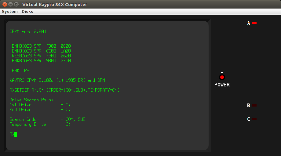
Look for disk image "drm-cpm310.logdisk" (mount in drive A and boot) on the downloads page, along with config file "kaypro84e". Additional CP/M 3 distro files are in disk image "cpm3-extra.logdisk".
CAUTION: Running Kaypro-specific programs under this version of CP/M 3 can be risky. CP/M 3 does not use the ROM BIOS (in order to avoid the cost of the high memory being consumed by it), and so anything that calls the ROM while CP/M 3 is loaded and running may corrupt the high memory parts of CP/M 3. It is not known exactly which Kaypro programs call the ROM directly, but one suspicious one is MITE (MITE.COM, MINSTALL.COM, AUTOMITE.COM). Standard CP/M programs should be fine.
I acquired some 256Kx1 DRAM chips, which were pin-compatible with the existing 64Kx1 chips on the board, having one new pin for the extra 2 address signals (DRAM of the era multiplexed address lines using CAS and RAS signals). I then added a 8-bit output port at (unused) I/O address 0x3c-0x3f. The top 4 bits fed into a comparator circuit that was used to select the "common page boundary". Bits 2, 3 were used to select the WR bank and bits 0, 1 were the RD bank - allowing direct inter-bank copies. Each of these pairs of address bits were multiplexed using CAS/RAS and then selected based on memory RD or WR and fed to the new address pin on the 256K DRAM chips (previously unused pin). That provided a simple, but flexible and powerful (for that era), memory management unit. Based on information currently available, here is the schematic for the modification. The MMU port bits are defined as follows:
| 7 | 6 | 5 | 4 | 3 | 2 | 1 | 0 |
|---|---|---|---|---|---|---|---|
| Comm Boundary | WR Bank | RD Bank | |||||
The following table describes how common page boundary was selected. Common page is always bank 0. Banked page can be any of bank 0-3, selected by WR bank and RD bank.
| 7 | 6 | 5 | 4 | Boundary | Banked Size | Comm Size |
|---|---|---|---|---|---|---|
| 1 | 1 | 1 | 1 | F000 | 60K | 4K |
| 1 | 1 | 1 | 0 | E000 | 56K | 8K |
| 1 | 1 | 0 | 1 | D000 | 52K | 12K |
| 1 | 1 | 0 | 0 | C000 | 48K | 16K |
| 1 | 0 | 1 | 1 | B000 | 44K | 20K |
| 1 | 0 | 1 | 0 | A000 | 40K | 24K |
| 1 | 0 | 0 | 1 | 9000 | 36K | 28K |
| 1 | 0 | 0 | 0 | 8000 | 32K | 32K |
| 0 | 1 | 1 | 1 | 7000 | 28K | 36K |
| 0 | 1 | 1 | 0 | 6000 | 24K | 40K |
| 0 | 1 | 0 | 1 | 5000 | 20K | 44K |
| 0 | 1 | 0 | 0 | 4000 | 16K | 48K |
| 0 | 0 | 1 | 1 | 3000 | 12K | 52K |
| 0 | 0 | 1 | 0 | 2000 | 8K | 56K |
| 0 | 0 | 0 | 1 | 1000 | 4K | 60K |
| 0 | 0 | 0 | 0 | 0000 | 0K | 64K |
The above memory arrangements all result in some wasted memory, as the memory above the common page boundary in banks other than "0" could not be accessed. But, it divided memory up into 4 banks that could be easily used to implement CP/M Plus (CP/M 3) or MP/M-II.
NOTE: for direct bank-to-bank copies, the code doing the copy must still be in common memory (at the absolute least must reside in the RD bank).
The modification for more than 2 floppies was a bit simpler. It involved adding a decoder IC to the existing 2 floppy select bits, turning the former into a 4-way select. Some additional circuitry was added, as I recall, to help avoid potential multiple select. I only had one extra drive, so the prior "no drives selected" state still resulted in no drive being selected.
The original mainboard was only partially populated, missing at least the modem and RTC chips (possibly the Z80-IPO also). I added the RTC (and PIO) so that CP/M Plus could have a time source.
To simplify the initial version, the ROM BIOS was not used at all. There are provisions in the code to use the ROM for the CRT, which would reduce the size of the BNKBIOS, but that was not tested.
The basic structure of the software is based on Magnolia Microsystem's CP/M Plus implementations, using a BNKBIOS made up of linkable modules (.REL files as produced by RMAC). It also supported several diskette formats from the H89 realm (without the need for patching the OS with MFDISK).